Semi-Conductor
Plasma Processes’ specialized, highly-engineered coatings and components are in high demand in the semiconductor industry due to the harsh environments required in crystal, semiconductor and wafer manufacturing. Harsh environments dramatically shorten the life of housing chambers and components, threatening the quality of the highly sensitive products.
Crystal Growth Crucibles and Accessories
Seed holders 4Plasma Processes fabricates high-purity, seamless refractory and platinum group metal crucibles and related components used in the manufacture of metal oxide single crystals including sapphire and YAG. Typical metals of fabrication include iridium, rhenium and tungsten with a wide range of diameters, heights and wall thicknesses available. Custom crucibles featuring complex geometries and multiple layers of different materials are also available. All crucibles can be refined to recover the precious metal.


Dielectric Coatings
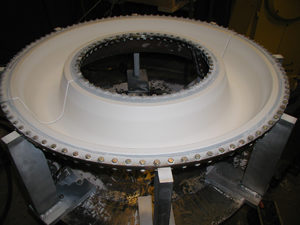
The electrical resistance of a coating can be the single most important factor during wafer processing or LCD glass preparation in determining fab output quality. A high quality coating can inhibit substrate corrosion and reduce downtime and expensive component replacement.
Sputter Targets
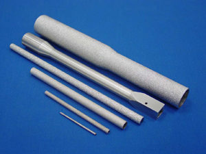
Cylindrical sputter target 2 Plasma Processes fabricates customized planar and cylindrical sputter targets in virtually any material composition desired. Cylindrical targets are available up to 52” in length.
